- 您现在的位置:买卖IC网 > Sheet目录356 > SC668ULTRT (Semtech)IC LED DRVR LMU 8CH MLPQUT20
�� �
�
�SC668�
�Register� Map� (continued)�
�Table� 22� —� ALS� Function� Enable� Bits�
�AD_AUTO� AD_EN�
�Comments�
�0�
�0�
�0�
�1�
�ADC� is� disabled.� Bank� #1� will� not� change�
�brightness� with� ambient� conditions.�
�ADC� is� enabled.� ADC� output� is� stored� in� the�
�AD� OUT� register.� Bank� #1� does� not� respond�
�to� the� AD� OUT� value.�
�AD� OUT� <� AD� RISE�
�AD_AUTO� =� 1� or� 0�
�Bank� #1� Brightness�
�=� Value� of� Register� 02h�
�1�
�0�
�ADC� is� disabled.� Bank� #1� current� is� set� to�
�the� start� or� target� current.� AD� OUT� is� com-�
�pared� to� AD� RISE� and� AD� FALL� registers.� A� new�
�value� may� be� written� to� AD� OUT� via� the� I� 2� C�
�interface.�
�AD_AUTO� =� 1�
�AD� OUT� <� AD� FALL�
�AD_AUTO� =� 0�
�AD� OUT� <� AD� FALL�
�AD_AUTO� =� 0�
�AD� OUT� >� AD� RISE�
�AD_AUTO� =� 1�
�AD� OUT� >� AD� RISE�
�1�
�1�
�ADC� is� enabled.� Bank� #1� current� is� set� to�
�the� start� or� target� current.� AD� OUT� is� com-�
�pared� to� AD� RISE� and� AD� FALL� registers.�
�Bank� #1� Brightness�
�=� Value� of� Register� 06h�
�The� ALS� comparator� functions� are� shown� in� Table� 23.�
�Table� 23� —� ALS� Comparator� Function� (1)�
�AD� OUT� >� AD� FALL�
�AD_AUTO� =� 1� or� 0�
�Conditions�
�AD� OUT� Effect� on� Bank� #1�
�AD� OUT� >� AD� RISE�
�Brightness� changes� to� target� value�
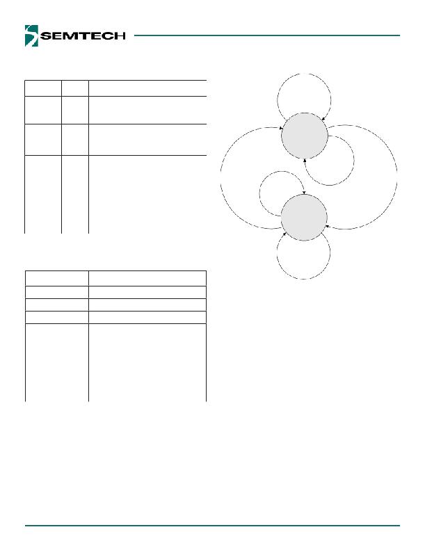
�Figure� 29� —� ADC� function� at� Bank� #1� Brightness�
�AD� OUT� <� AD� FALL� Brightness� changes� to� start� value�
�AD� FALL� ≤� AD� OUT� ≤� AD� RISE� Brightness� does� not� change�
�Hysteresis� between� the� rising� and� falling�
�thresholds� is� disabled,� and� .� .� .�
�AD� FALL� →� has� no� effect� on� brightness�
�AD� O� >� AD� RISE� →� brightness� changes� to�
�AD� FALL� ≥� AD� RISE� target� value�
�AD� O� <� AD� RISE� →� brightness� changes� to�
�start� value�
�AD� O� =� AD� RISE� →� brightness� does� not�
�change�
�Notes:�
�1)� When� AD_AUTO� bit� is� high.�
�The� state� diagram� of� Figure� 29� shows� how� the� ADC� is� used�
�to� change� the� brightness� of� backlight� bank� #1.� No� auto-�
�matic� change� in� brightness� occurs� when� AD_AUTO� =� 0.�
�ADC� Output� and� Threshold� Register� (13h)�
�This� register� contains� the� value� AD� OUT� which� is� compared�
�with� AD� RISE� and� AD� FALL� .� The� contents� of� AD� OUT� may� originate�
�automatically� from� the� ADC,� when� the� AD_EN� bit� is� a� logic�
�one.� Alternatively,� AD� OUT� may� be� written� to� the� register� via�
�the� I� 2� C� interface� when� the� AD_EN� bit� is� a� logic� zero.�
�When� AD_EN� =� 1,� the� ADC� receives� its� analog� voltage�
�input� signal� from� the� external� photo-detector� circuit� con-�
�nected� to� the� ADI� pin.� V� ADI� is� then� converted� into� digital�
�and� stored� as� the� 8� bit� word� AD� OUT� .� The� reference� voltage�
�for� the� ADC� is� provided� internally� by� the� output� of� LDO4�
�(V� LDO4� ).� When� the� voltage� V� ADI� is� equal� to� V� LDO4� ,� the� ADC� is�
�at� full-scale� value� FFh,� and� AD� OUT� will� equal� FFh.�
�When� using� an� external� photo-detection� circuit,� the� ADC�
�requires� the� LDO� output� voltage� V� LDO4� to� remain� constant.�
�V� LDO4� can� drop-out� if� the� supply� voltage� becomes� too� low.�
�V� LDO4� should� be� set� to� a� value� sufficiently� low� to� guard�
�against� drop-out.�
�41�
�发布紧急采购,3分钟左右您将得到回复。
相关PDF资料
SDIN2B2-8G
IC INAND FLASH 8GB 169FBGA
SDK-DM3730-10-256512R
KIT DEV ZOOM FOR AM/DM37X
SDK-DM3730-20-256512R
KIT DEV ZOOM FOR AM/DM37X
SE162216
ENCLOSURE ASSY 6U X 19" X 16"
SF-2194
RACK SWING FRAME 38"X21.25" BLK
SF-2294
RACK SWING FRAME 35" X 19"
SFD1200-12BG
FRONT END DC/DC 1200W 12V
SFH21-PPPN-D07-ID-BK-M181
CONN RECEPT 14POS 2MM IDT GOLD
相关代理商/技术参数
SC-67
制造商:JIFFY 功能描述:CORRUGATED BOX DW 24X18X18 PK15 制造商:JIFFY 功能描述:CORRUGATED BOX, DW, 24X18X18, PK15
SC6750
制造商:Alltrade Tools LLC 功能描述:COMB. SET
SC68253LK081
制造商:ON Semiconductor 功能描述:
SC68253PK073
制造商:Rochester Electronics LLC 功能描述:- Bulk
SC68254DW154R2
制造商:Rochester Electronics LLC 功能描述:- Bulk
SC68254PK4538
制造商:ON Semiconductor 功能描述:
SC68255DWT373R2
制造商:ON Semiconductor 功能描述:
SC68285PK195A
制造商:ON Semiconductor 功能描述: